1 / 7
Apr 2018

I thought I saw this asked before, but can’t seem to find it now. Is there any method to mark a “keep-out” area for applying the paste? We have a board that we have already placed and flowed, and then discovered that a large chip was placed one-pin off. We have removed it and cleaned it, and would like to just repaste it on the Voltera. However, we have to make sure that the Voltera avoids the areas with placed parts.

Any thoughts on present or future solutions?

  • created

    Apr '18
  • last reply

    Apr '18
  • 6

    replies

  • 1.7k

    views

  • 4

    users

  • 2

    likes

  • 2

    links

Hi Gary, did you try to “keep out” those areas directly with eagle or kikad, and running after the cam processor to get the special files for keeping out. Just be aware for renaming the filename before…

We haven’t yet tried anything. The module is on one side of the board, but there are parts all around it. So even if we limit the Gerber to just that section, which we can easily do, that doesn’t give me confidence that the pathway the Voltera takes will not have it run into existing IC’s or headers on the board. Before I try it, I would like some guarantee that the pathway is safe.

@Gary - Perhaps make a mockup board, no parts but draw on it the areas you need to keep out of, and watch what happens? I’d probably do this even if you had a “guaranteed keep out” region, just to make sure on the first run, rather than risking breaking a nozzle or worse.

That’s a good idea. We can try that. Still would like to know if there is a current or future plan in the software to do this. (and orient the Gerber as well).

If not already there then it is a definite have-to-have feature!
It has been in the issue request thread since October 2016, the team was planning to look into implementing it after some current issues back then were addressed.

Hey @Gary,

There is currently no ability to probe a subset of the board.

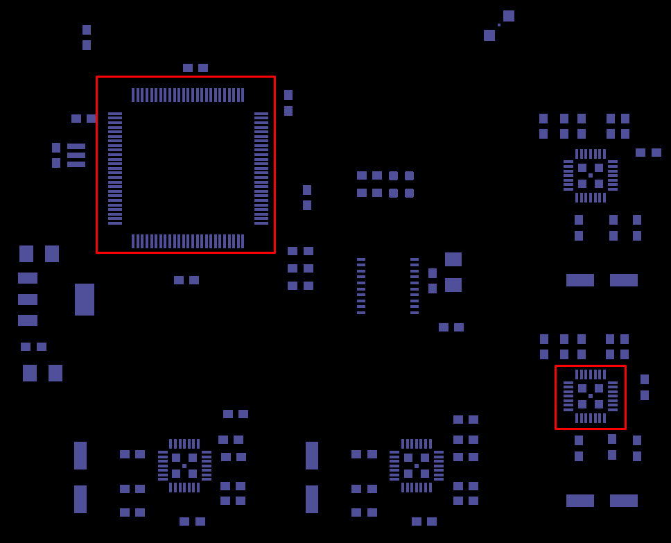
If your Gerber file contains all of the pads in the board, then the software will probe enough points to create a map of the entire board. This basically guarantees the probe will crash into a component if your board is partially assembled.

The ability to block out portions of your Gerber as soon as the file is loaded is on our to-do list, but it hasn’t been prioritized yet.

A workwaround is to load the Gerber file in a program like Gerbv2 and delete the pads that you do not want to probe and then load that modified file in the voltera software. (watch out - there is no ‘Undo’ in Gerbv)

Warning: This approach works if you do one IC at a time. The probe only raises about 0.5mm between probe points.

Example: Let’s assume I have dispensed paste and assembled the following board, and for whatever reason I need to dispense paste on the following pads again.

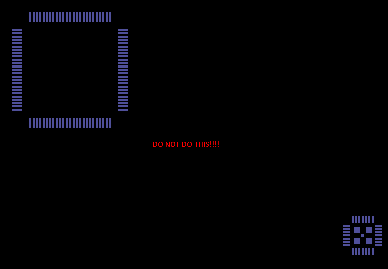
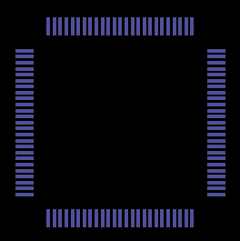
I would delete all the pads I do not need in Gerbv and get 2 files. My first file:

image

My second file:

image

Do NOT load a file that has both ICs.

Why? When the probe finishes mapping one IC it will follow a straight path towards the second IC - crashing into the soldered components.

Does that make sense?