1 / 15
Sep 2016

Hi Everyone!

We just released software version 0.6.2. We're incredibly excited about these features and wanted to let you know all about them

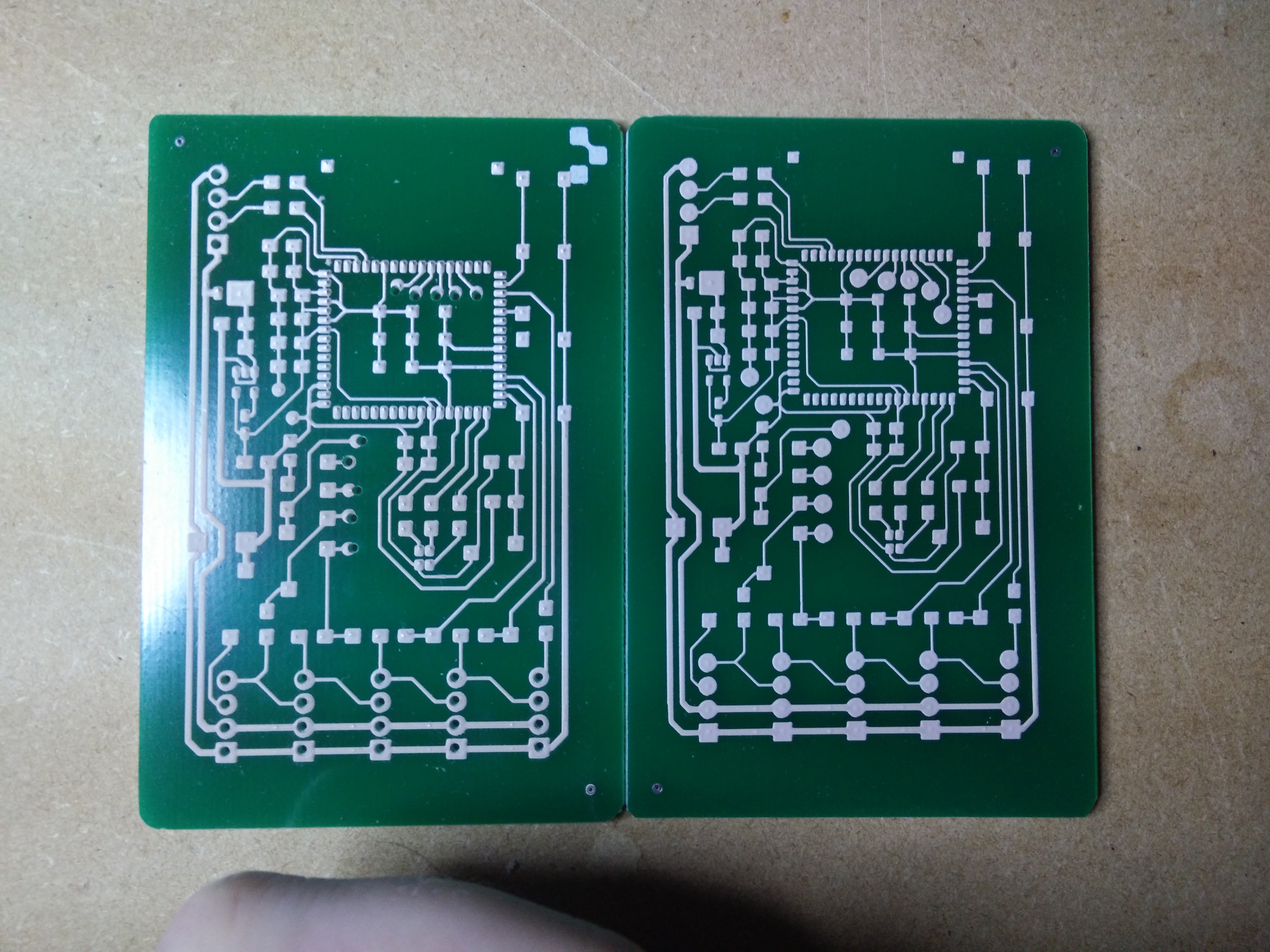
Double Sided Printing

Finally, it's here! (@emcniece, @lintilla, @DavidYon47)

The next time you print a circuit, you will have to choose between a simple or an aligned print.

A simple print will let you position the circuit wherever you want. You will be able to click and drag the circuit around to place it somewhere on the substrate. (This was the standard behaviour before v0.6.0)

An aligned print will let you position the circuit by identifying two key features on the board. Just like in solder paste dispensing, the location of two points needs to be measured using the arrow keys.

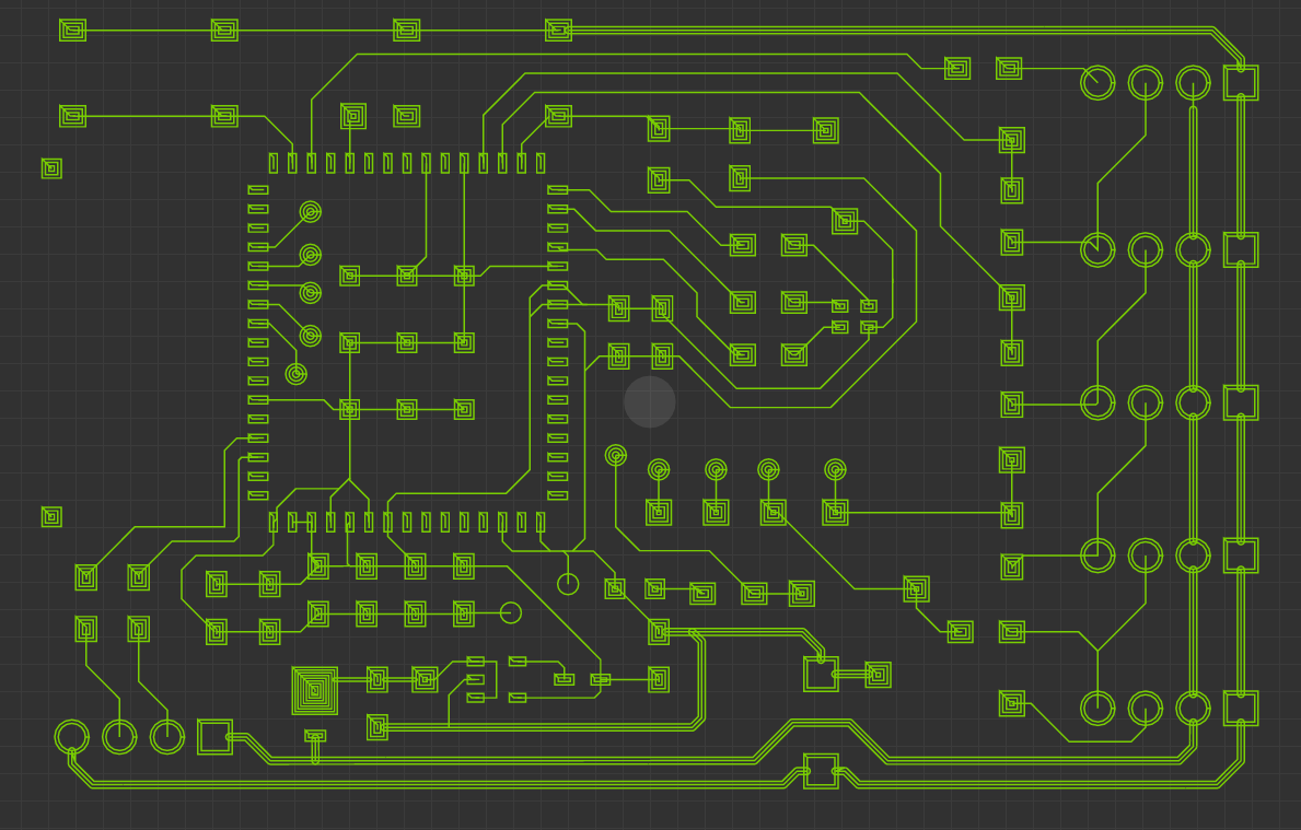
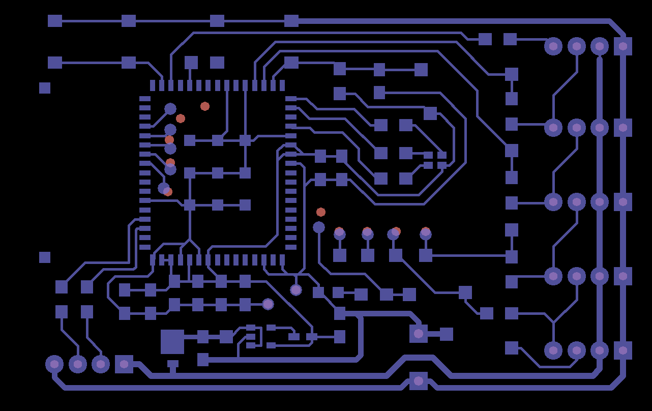
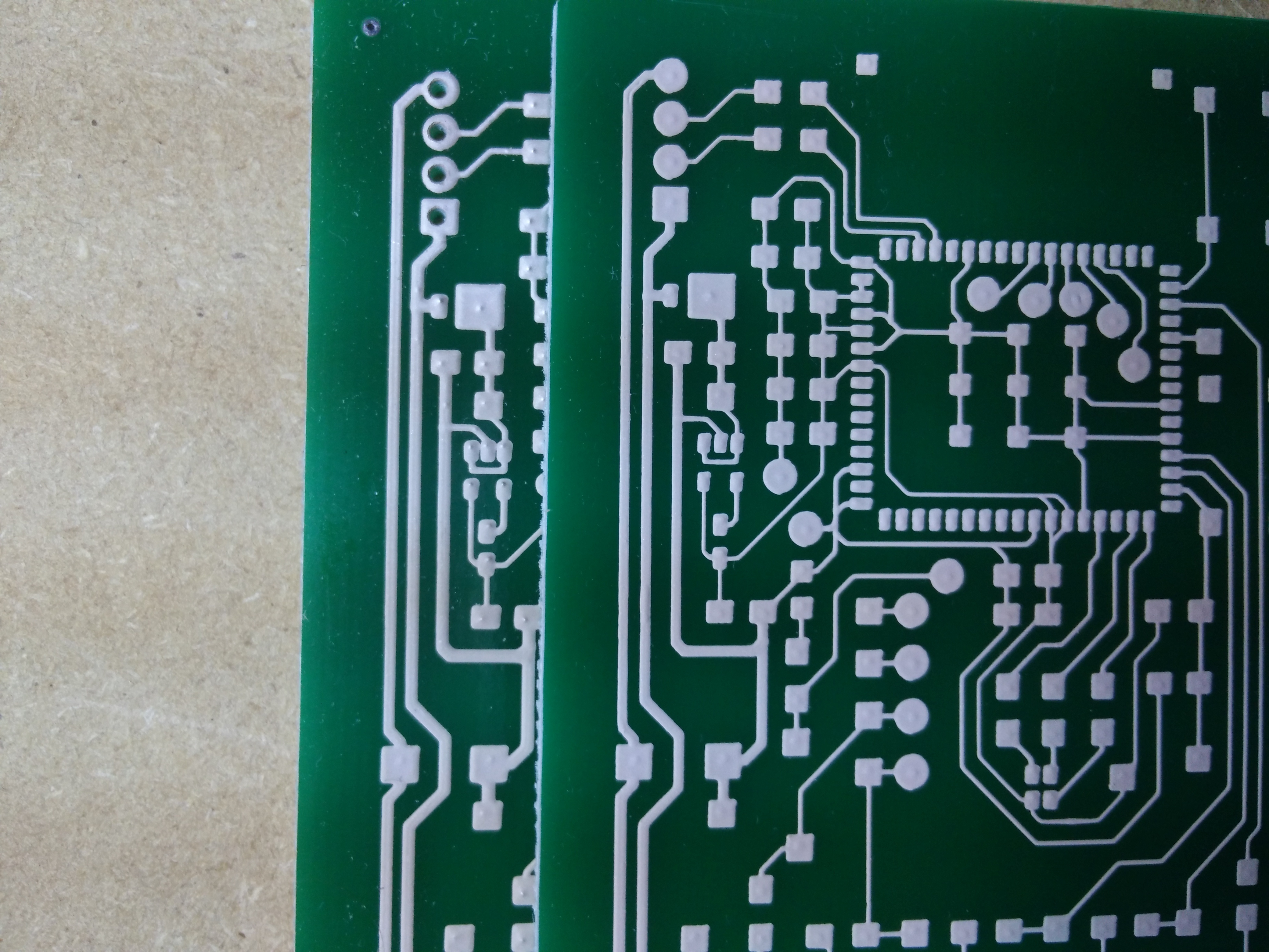
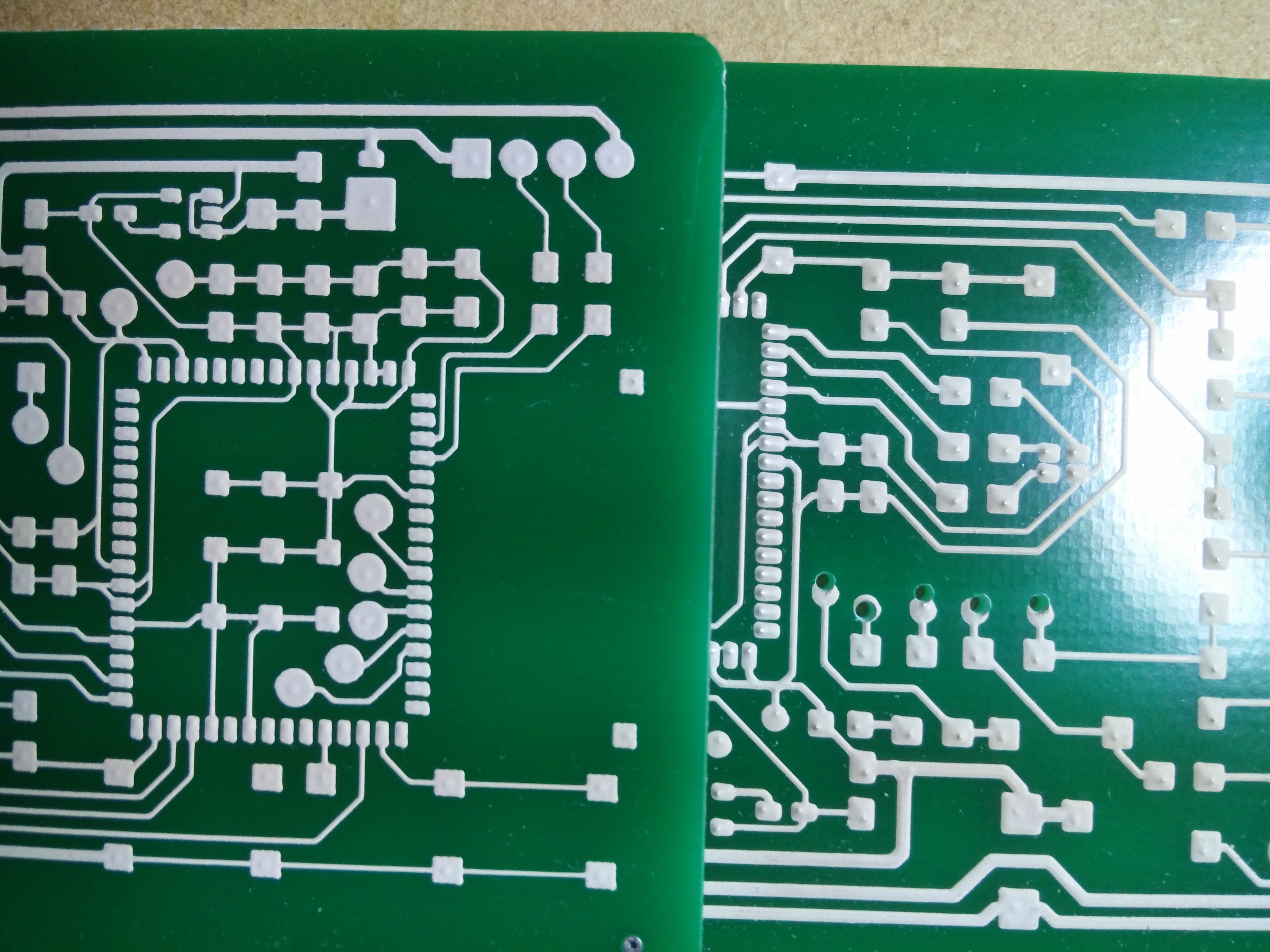
Important: For alignment purposes, the software will pick the two smallest pads that are farthest apart. It gives priority to pads with holes (thru holes or vias), followed by regular pads (SMT pads), followed by traces.

A double sided circuit consists of two separate prints: A simple print followed by an aligned print. During an aligned print you will have to locate the position of two holes. A user guide on double sided printing will be posted here22.

Faster Printing

Over the past few weeks we've been experimenting with faster printing speeds. We realized we could increase the printing speed by 66% without any negative effects.

A Hello World circuit now takes 3 minutes and 22 seconds to print! The software will automatically start using the faster print speed once it updates.

Less ink in pads

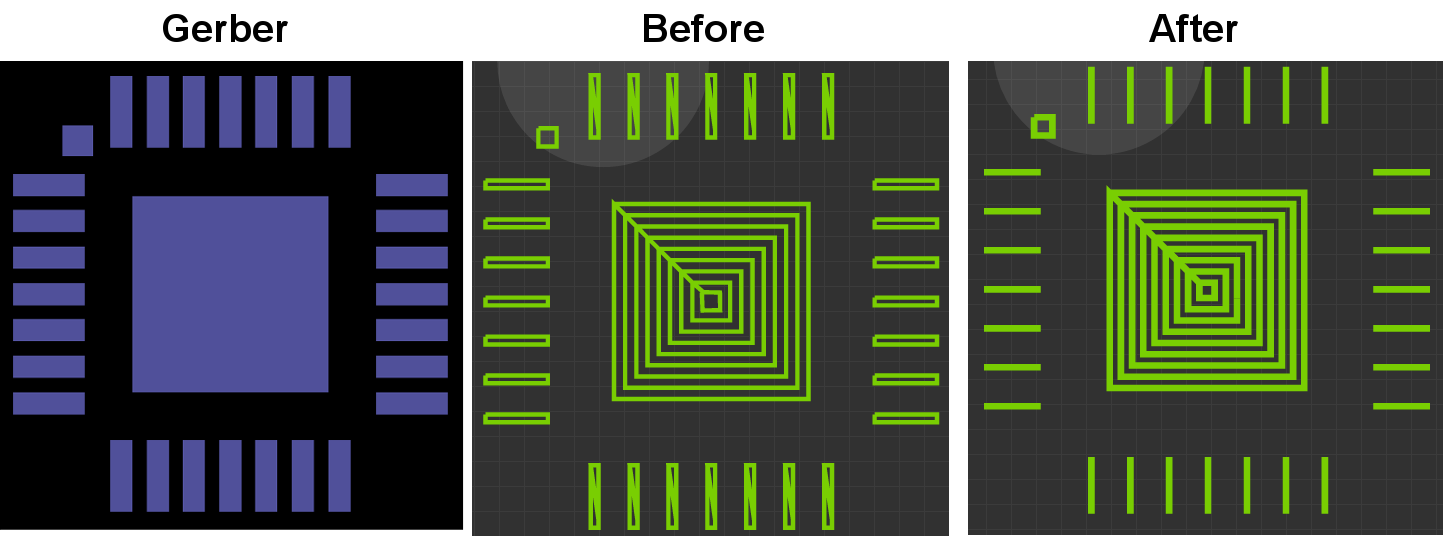
Several of you have noticed the 'dimples' that are left behind at the center of the pads when the nozzle raises. It is hard to eliminate them altogether, but they tend to be exaggerated when too much ink is dispensed in one area. We have modified the software so that the innermost pass of the pad can now be a line instead of forcing it to be a rectangle. This will reduce over-filling and should lead to more uniform pads. (@Don)

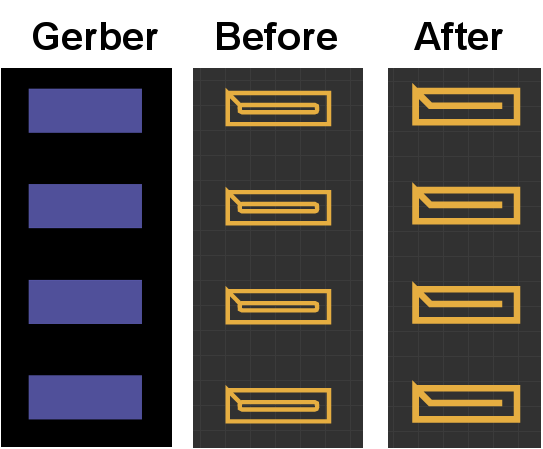
Fun fact: Here at Voltera HQ we call the 'dimple' a 'kiss'. (like a Hershey Kiss)

Similarly, very small thin pads will now be drawn as a single line, instead of a rectangle, this will help reduce the risk of shorting if you are printing fine pitch ICs.

Other

  • We have added Alt+C as a shortcut to bring up the console. This shortcut is more accessible in international keyboards and is more in line with the other shortcuts (like Alt + R, Alt + H). Thanks @Eriond for the tip!
  • Release notes have been added to the app, when the app is updated they will be displayed automatically so you can stay in the loop.
  • Previously, if you had rectangular pads with rounded corners the software would not be able to process them and would render a circle instead. We've patched the issue now.

That is it for now, but if you have general feedback, questions or feature requests, please comment below.

Cheers,
Jesus Zozaya

  • created

    Sep '16
  • last reply

    Sep '16
  • 14

    replies

  • 5.5k

    views

  • 4

    users

  • 8

    likes

  • 7

    links

Its so nice to see how you really listen to the community and (as far as possible) implement our suggestions. We humbly thank you, :hugging:

Looking good... really good.

I have printed 7 boards so far, tweaking settings each time. Today's update (0.6.2 up from 0.5) really changed the ink flow. Previously I was dialing the flow rate to -18 and manually reducing to -22 when pads were being printed, and there was still significant make-out sessions happening. Today the flow was only -8 and anything lower resulted in broken traces.

For the following images, yesterday's board is on the left and today's board is on the right!

That's the smallest drill bit I have available: 66Y. I enlarged vias to 2mm diameter for today so that I can drill them with room to spare.

Note the SOT23-5 package on the left side, vertical centerish - today's print is WAY cleaner, and I didn't have to intervene with flow adjustment.

This last image has the boards flipped, oops - the drilled board is the old one. Come to think of it, I should have tried for an elevation shot to demonstrate the difference in pad height, as it is definitely noticeable.

My off-center via drilling is a result of trying to figure out via diameter with my huge drill bit. I am using Kicad, and I'm not sure exactly why the vias (and through-hole pads) aren't being left hollow. Are they supposed to get filled in? If you're interested in investigating, the code is available over here4. Kicad exports drill files as *.drl which is only a little annoying because I have to rename them to *.txt to get the software to recognize them.

Anyway, great work! I am finally at a point where I can solder and populate a board, so that might happen tonight :smile:

Hi @emcniece,

What an improvement! Love those side by side comparisons - thanks for sharing.

It definitely doesn't look like the software recognized the holes at all. The software should have compensated and printed 'donuts' on all the pads that have a hole. Like so:

.


I'll take a look at the *.DRL file and get back to you.
Jesus Zozaya

pinned Sep 1, '16

Just attempted an aligned print, and the height probe stage failed. The probe descended too far into a drilled via, didn't retract far enough, continued its X/Y movement, got caught inside the edge of the via, retracted further, went WAY off-board, probed the hot plate, then halted with an error.

We don't have instructions at the user guide1 yet, so I followed the Youtube video8:

  1. Print front copper, bake
  2. Drill holes
  3. Tape front copper side
  4. Fill vias by hand from bottom layer, wipe excess
  5. Clamp & align
  6. Height probe <- fail point
  7. Dispense bottom layer ink, bake

The height probe was going well up until the last via probe - it probed the outer corners of the farthest pads, then did the board centers along the edges, then it probed around the edges of a few vias... and then it dipped straight into one of the middle vias and got caught. I have a feeling that this may have been caused by the size of my drills - I just measured my bit to be 0.8mm diameter.

There doesn't appear to be any damage to the probe, but visual inspection is only so good. Not really feeling confident enough to proceed with an ink print as my only good tip is on the ink cartridge, the solder tip is already bent, and the other 3 tips are broken. I think my next batch of tips arrives next week sometime :cry:

The code is still available on Github6, with a freshly generated bottom layer. The drill file still doesn't seem to be doing anything, perhaps the lack of holes is messing the probe sequence up?

I closed the error dialog too soon, but here's a console dump:

 <  ok
83 > V02 Z1 F200
   <  empty
   <  positionUpdate x:28.395999 y:118.872001 z:-0.510000 e:0.000000
   <  ok
83 > V1 X28.595 Y119.161 F12000
   <  ok
83 > V4
   <  probeMeasurement x:28.595 y:119.161 z:-0.165
   <  ok
83 > V02 Z1 F200
   <  empty
   <  ok
83 > V1 X28.888 Y119.352 F12000
   <  ok
83 > V4
   <  probeMeasurement x:28.888 y:119.352 z:-0.165
   <  ok
83 > V02 Z1 F200
   <  empty
   <  positionUpdate x:28.888000 y:119.352005 z:-0.511875 e:0.000000
   <  ok
83 > V1 X29.233 Y119.416 F12000
   <  ok
83 > V4
   <  probeMeasurement x:29.233 y:119.416 z:-0.164
   <  ok
83 > V02 Z1 F200
   <  empty
   <  positionUpdate x:29.232999 y:119.416007 z:-0.510625 e:0.000000
   <  ok
83 > V1 X67.603 Y120.712 F12000
   <  ok
83 > V4
   <  probeMeasurement x:67.603 y:120.712 z:-0.141
   <  ok
83 > V02 Z1 F200
   <  empty
   <  positionUpdate x:67.602996 y:120.711997 z:-0.488125 e:0.000000
   <  ok
83 > V1 X69.402 Y120.689 F12000
   <  ok
83 > V4
   <  probeMeasurement x:69.402 y:120.689 z:-0.146
   <  ok
83 > V02 Z1 F200
   <  empty
   <  positionUpdate x:69.402000 y:120.689002 z:-0.492500 e:0.000000
   <  ok
83 > V1 X35.809156487229274 Y117.53283751592198 F12000
   <  ok
83 > V4
   <  probeMeasurement x:35.809 y:117.533 z:-0.129
   <  ok
83 > V02 Z1 F200
   <  empty
   <  positionUpdate x:35.809158 y:117.532836 z:-0.476250 e:0.000000
   <  ok
83 > V1 X86.34519597087699 Y116.28023330580606 F12000
   <  ok
83 > V4
   <  probeMeasurement x:86.345 y:116.280 z:-0.168
   <  ok
83 > V02 Z1 F200
   <  empty
   <  positionUpdate x:86.345191 y:116.280227 z:-0.514375 e:0.000000
   <  ok
83 > V1 X67.51453721256954 Y113.83366280239147 F12000
   <  ok
83 > V4
   <  probeMeasurement x:67.515 y:113.834 z:-0.093
   <  ok
83 > V02 Z1 F200
   <  empty
   <  positionUpdate x:67.514533 y:113.833671 z:-0.440000 e:0.000000
   <  ok
83 > V1 X55.11586717219832 Y110.18294482780048 F12000
   <  ok
83 > V4
   <  probeMeasurement x:55.116 y:110.183 z:-1.300
   <  ok
83 > V02 Z1 F200
   <  empty
   <  positionUpdate x:55.115863 y:110.182945 z:-1.646875 e:0.000000
   <  ok
83 > V1 X86.24190338168323 Y108.28090016853659 F12000
   <  ok
83 > V4
   <  probeMeasurement x:86.242 y:108.281 z:-0.619
   <  ok
83 > V02 Z1 F200
   <  empty
   <  positionUpdate x:86.241897 y:108.280883 z:-0.965625 e:0.000000
   <  ok
83 > V1 X56.81830067592339 Y104.20567199478698 F12000
   <  ok
83 > V4
   <  probeMeasurement x:56.818 y:104.206 z:-0.254
   <  ok
83 > V02 Z1 F200
   <  empty
   <  positionUpdate x:56.818298 y:104.205665 z:-0.600625 e:0.000000
   <  bedTemperatureUpdate current:33.5 target:0.0 timeRemaining:0.0
   <  ok
83 > V1 X69.03335724842984 Y103.7027079511117 F12000
   <  ok
83 > V4
   <  probeMeasurement x:69.033 y:103.703 z:-0.218
   <  ok
83 > V02 Z1 F200
   <  empty
   <  ok
83 > V1 X62.70866298025649 Y103.75947443889588 F12000
   <  ok
83 > V4
   <  probeMeasurement x:62.709 y:103.759 z:-0.235
   <  ok
83 > V02 Z1 F200
   <  empty
   <  positionUpdate x:62.708660 y:103.759460 z:-0.581875 e:0.000000
   <  bedTemperatureUpdate current:26.0 target:0.0 timeRemaining:0.0
   <  ok
83 > V1 X46.815092904338755 Y101.88942955657556 F12000
   <  ok
83 > V4
   <  probeMeasurement x:46.815 y:101.889 z:-1.936
   <  ok
83 > V02 Z1 F200
   <  empty
   <  positionUpdate x:46.815093 y:101.889427 z:-2.283125 e:0.000000
   <  ok
83 > V1 X52.24329038379351 Y101.81933714228472 F12000
   <  ok
83 > V4
   <  probeMeasurement x:52.243 y:101.819 z:-1.953
   <  ok
83 > V02 Z1 F200
   <  empty
   <  ok
83 > V1 X86.13861079248947 Y100.2815670312671 F12000
   <  ok
83 > V4
   <  positionUpdate x:86.138603 y:100.281562 z:-1.299375 e:0.000000
   <  probeMeasurement x:86.139 y:100.282 z:-1.319
   <  ok
83 > V02 Z1 F200
   <  empty
   <  ok
83 > V1 X41.205475535121934 Y99.78668326399035 F12000
   <  ok
83 > V4
   <  probeMeasurement x:41.205 y:99.787 z:-1.809
   <  ok
83 > V02 Z1 F200
   <  homedStatusUpdate x:0 y:-1 z:-1
   <  homedStatusUpdate x:0 y:0 z:-1
   <  homedStatusUpdate x:0 y:0 z:0
   <  Error:Unable to complete movement, limit switch triggered. Motion stopped at x:60.82
   <  empty
   <  positionUpdate x:41.205474 y:99.786674 z:-2.155625 e:0.000000
   <  homedStatusUpdate x:0 y:-1 z:0
   <  homedStatusUpdate x:-1 y:-1 z:0
   <  homedStatusUpdate x:-1 y:-1 z:-1
   <  Error:Unable to move to 12.20 in Z-axis, position falls outside of safe bounds
   <  ok
   <  positionUpdate x:32.071189 y:3.543333 z:11.200626 e:0.000000
84 > V3 Z
   <  ok
84 > V1 X90.024 Y83.48 F12000
   <  ok
84 > M400
   <  ok
   <  empty
   <  positionUpdate x:90.024002 y:83.479995 z:11.201251 e:0.000000
85 > V1 F12000
   <  ok
85 > V4
   <  probeMeasurement x:90.024 y:83.480 z:-1.180
   <  ok
85 > V02 Z0.6 F200
   <  positionUpdate x:90.024002 y:83.479995 z:-1.536875 e:0.000000
   <  ok
85 > M400
   <  ok
   <  empty
   <  positionUpdate x:90.024002 y:83.479995 z:-0.936875 e:0.000000
86 > V3 Z
   <  ok
86 > M400
   <  positionUpdate x:90.024002 y:83.479995 z:11.200626 e:0.000000
   <  ok
   <  echo:The stepper has been inactive for more than 300000ms, deactivating motors
   <  homedStatusUpdate x:0 y:-1 z:-1
   <  homedStatusUpdate x:0 y:0 z:-1
   <  homedStatusUpdate x:0 y:0 z:0
   <  echo:The stepper has been inactive for more than 300000ms, deactivating motors
   <  bedTemperatureUpdate current:26.5 target:0.0 timeRemaining:0.0
   <  echo:The stepper has been inactive for more than 300000ms, deactivating motors
   <  echo:The stepper has been inactive for more than 300000ms, deactivating motors
   <  echo:The stepper has been inactive for more than 300000ms, deactivating motors

Hey @emcniece ,

I'm impressed to see that you're blazing the trail for double-sided printing, even without support docs! The user guides section for the aligned printing feature is in progress and should be released soon, but the approach that you were taking is exactly the process we follow.

You're right that the missing drill locations are causing the probing problem. The V-one software will purposely avoid drills and holes when probing, to prevent running into the exact issue you saw - without these locations, it won't know whether it is probing a via or just another pad (which would be safe typically).

It's quite unlikely that the probe is damaged, so you should be able to pick up where you left off as soon as we're able to resolve the problem with processing the .drl file - Jesus will be in touch as soon as we have a solution!

  • Matt

Awesome, thanks @mewertow! I extracted the app to see what the drill file looked like for the Hello World example, but of course it's a single-layer board and as such it only has GTL and GTP files. Maybe we can whip up a 2-layer Hello World to give users the full tutorial :wink:

Hi @emcniece,

I managed - to get your files working.

It seems that in KiCad, the coordinate origin is in the top left (?), so the Y axis coordinates for the drills all had negative values and we didn't take this into account. You'll notice that the drills are now compensated for in the software as expected.

However looking at the files with a Gerber viewer, it looks like some drills are not dead center in the pads. Most are fine, but there's a couple that are overlapping with pads and some that are not touching at all

Is this intentional?

I ask because at the moment the software only compensates for holes only if the hole is completely enveloped by a pad. That's why you'll see some holes missing in the previous image.

The fix will be rolled out in the next SW version.


Enjoy your long weekend!
Jesus Zozaya

That is excellent, thank you for the troubleshooting help! I've made a few adjustments to the PCB - it looks like the drill marks are for the most recent board, and the PCB copper is the old version.

Kicad has an option to invert/mirror the Y axis during gerber/drill file generation. Doing this for the drill file results in the following:

M48
;DRILL file {KiCad 4.0.3-stable} date Friday, September 02, 2016 'PMt' 03:41:24 PM
;FORMAT={-:-/ absolute / metric / decimal}
FMAT,2
METRIC,TZ
T1C0.900
T2C1.000
T3C1.001
%
G90
G05
M71
T1
X156.Y107.
X158.5Y107.
X161.Y107.
X163.5Y107.
X209.75Y72.75
X209.75Y81.5
X209.75Y89.5
X209.75Y97.5
X209.75Y105.5
X212.25Y72.75
X212.25Y81.5
X212.25Y89.5
X212.25Y97.5
X212.25Y105.5
X214.75Y72.75
X214.75Y81.5
X214.75Y89.5
X214.75Y97.5
X214.75Y105.5
X217.25Y72.75
X217.25Y81.5
X217.25Y89.5
X217.25Y97.5
X217.25Y105.5
T2
X168.2Y88.4
X168.4Y82.8
X168.504Y85.296
X169.6Y80.5
X172.2Y79.2
X179.Y100.5
X182.Y99.
X184.7Y90.6
X186.7Y92.7
X189.7Y92.7
X192.8Y92.7
X196.Y92.7
T3
X195.25Y103.71
X195.25Y108.79
T0
M30

This is notably different from the top-origin plotting found at https://github.com/emcniece/lamply-circuit/blob/master/Lamply.drl5. Should Kicad users be mirroring the Y-axis?

And finally, what gerber viewer do you use? Thanks again for the help!

Just confirming that mirroring y-axis during Kicad drill file export does not get the V1 software to recognize the drills in the correct locations.

http://viewer.tracespace.io/6 is pretty useful for viewing gerbers and drill hole alignment!

Feature request: Holes filetype addition in app/modules/loadCircuit/gerbers.js:

export const GerberExtensions = {
  Top: ['GTL', 'gbr', 'top', 'cmp'],
  Bottom: ['GBL', 'gbl', 'bottom', 'sol'],
  Solder: ['GTP', 'GBP', 'sts'],
  Holes: ['txt', 'drl', 'DRL']
};

Sadly, I can't webpack and test the app - app/modules/vOne/tools directory is missing :smile:

Hi @emcniece,

That should not be necessary after the next SW update. As long as the origin location between the Gerbers and the drill file matches it should render fine.

We use Gerbv4 to view gerber files. Its feature set is quite limited (you can't copy or paste traces/pads) but it has proven to be super useful for us.

We can add the *.DRL extension no problem.

psst @mewertow - what do you think the ETA is on the next software update? Just received a box of new tips, pretty stoked to get soldering again!

@emcniece You won't have to wait long! The software team is putting the next update through release testing right now, so you should be good to go real soon. I'll make sure to notify the thread as soon as it's out :slight_smile: